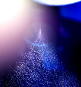
Tapping and wiping can only work on flexible devices, when flexible materials are used for touchscreens and electric circuits, but not brittle materials like indium tin oxide or silicon. For this purpose, INM is working with the process of electrospinning, a technique that produces ultra-fine fibers.
Whole press release
Flexible, transparent, and conductive electrodes (FTCEs) are a key enabling technology for the new generation of flexible, printable and wearable electronics. The touchscreens and displays of the future will be curved and flexible and integrated into cars, phones, or medical technology. Tapping and wiping can only work on flexible devices, when flexible materials are used for touchscreens and electric circuits, but not brittle materials like indium tin oxide or silicon. For this purpose, INM – Leibniz Institute for New Materials is working with the process of electrospinning, a technique that produces ultra-fine fibers that are up to 100 times thinner than a human hair. These fibers are collected on glass or on foils in an unstructured, wide mesh net. When conductive materials are spun, flexible conductive transparent electrodes could be produced. These FTCEs have transparencies comparable to indium tin oxide with low haze less than two percent.
The developers will demonstrate this technique at stand B46 in hall 2 at this year’s Hannover Messe, which takes place from April 23 to 27.
Electrospinning relies on the electro-hydrodynamics of a polymer droplet in a strong electromagnetic field. The polymer droplet deforms into a cone under the electromagnetic field and ejects a jet of liquid polymer to reduce the charge on the droplet. Once in the air the polymer jet experiences a bending instability causing the fiber to whip through the air effectively drawing the fiber to diameters below 500 nanometers. The fibers are collected on glass or on a film in an unstructured, wide mesh net. “Our innovation lies in the choise of starting materials. We can use sols, which have to be calcined, or polymers and composites with no further heat treatment. Depending on the starting material, it is possible to produce both intrinsically conductive fibers and those which are electrically conductive in a further step via silvering,” explains Peter William de Oliveira, Head of the InnovationCenter INM.
In contrast to patterning processes via stamps or printing methods, electrospinning easily produces unstructured fiber networks with sufficient space between the fibers that light scattering is reduced to less than two percent. At the same time, the length of the fibers reduces both the number of fibers needed for conductivity with sufficient coverage and connections between the fibers which reduce the contact resistance. With fiber thicknesses well under 500 nanometers, the fibers are not visible to the human eye and appear transparent. The net-like, random nature of the fiber deposition also eliminates typical diffraction phenomena, such as distracting rainbow effects.
“This process is machine-compatible and therefore allows a very efficient path for the manufacture of such electrodes. At the InnovationCenter we have a spinning station with which we can meet the different needs of the interested parties,” says de Oliveira. For example, electrodes could be developed for flexible displays, for photo-voltaics or for passive sensors.
The fibers produced by electrospinning could not only be used as electrodes, but are also suitable to be woven into electronics, or to use them for active water treatment because of their high surface area and material properties.
Your expert at INM
Dr. Peter William de Oliveira
INM – Leibniz Institut for New Materials
Head Optical Materials
Head InnovationCenter INM
Tel: 0681-9300-148
[email protected]


