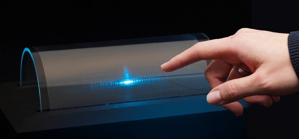
Flexible, transparent, and conductive electrodes are a key enabling technology for the new generation of flexible, printable and wearable electronics. The touchscreens and displays of the future will be curved and flexible and integrated into cars, phones, or medical technology. To allow typing and swiping even on curved smartphones, the touchscreens and electrical circuits on them have also to be curved and flexible. Therefore INM – Leibniz Institute for New Materials has developed several techniques that enable touchscreens and circuits on flexible foils.

The INM – Leibniz Institute for New Materials will show such coatings at this year’s LOPEC trade fair in Munich at booth 301 in hall B 0 from March 23-24 in a joint booth with the Nanoinitiative Bayern GmbH, Cluster Nanotechnology: The INM will present suitable coatings that can be produced cost-effectively using three different low-cost methods: With inkjet or gravure printing processes, with so-called electrospinning and with photo¬chemical metallization.
- INM presents layers produced by printing nanoparticle inks of transparent conducting oxides (TCOs) directly onto thin plastic films. By inkjet printing or gravure printing, transparent and flexible paths and structures are formed that are still electrically conductive even when the films are deformed. This enables the production of electrode structures in a cost-effective one-step printing process.
- Another method used by the INM is electrospinning on glass and also on foil. In this process, materials are spun into extremely fine fibers that are a hundred times thinner than human hair. These are deposited as an unstructured, wide-meshed network By spinning conductive materials, the results are transparent, flexible, conductive electrodes with a scattering loss of less than two percent. “The novelty of our approach lies in the starting materials we use. We process polymers and composites, but also sols, which are then calcined. Depending on the starting material, it is possible to produce both intrinsically conductive fibers and those that become electrically conductive in a further step via metallization,” explains Peter William de Oliveira, head of the program area Optical Materials and the Innovation Center at INM.
- In the third method, photochemical metallization, plastic films are coated with a photoactive layer of metal oxide nanoparticles. “We then apply a colorless, UV-stable silver compound,” Peter William de Oliveira explains, ” The irradiation of this sequence of layers by Ultraviolet light causes the silver compound to decompose at the photoactive layer and the silver ions are reduced to metallic, electrically conductive silver. This process can be used to form conductive tracks of different widths, down to a line width of one-thousandth of a millimeter.”
For the various functions of a touchscreen, the surfaces are equipped with microscopic, invisible conductor paths. In the edges of the devices, these microscopic tracks converge to form larger conductor paths. Until now, these different conductor paths had to be produced in complex processes involving several steps. Photochemical metallization now enables this to be accomplished in a single step on the flexible foils. The new process is fast, flexible, variable in size, cost-effective and environmentally friendly. Further process steps for post-treatment are not required.
Your expert at INM
Dr. Peter William de Oliveira
Head Optical Materials
Head InnovationCenter INM
Phone: +49681-9300-148
E-Mail: [email protected]

